Bipul Talukdar, Director of Applications Engineering for North America, SmartDV
EEWeb
November 9, 2021
A well-repeated truism throughout the semiconductor industry is that chip design verification is complex and often takes up the largest portion of a design project’s schedule –– sometimes as much as 70% –– and an ongoing challenge facing verification engineers. The all-important methodology is used throughout the chip design process and considered the gatekeeper at each stage of the process as the design transitions from a high-level description to detailed layout of the chip and ultimately to first silicon prototypes.
The last hurdle of any project before committing to volume manufacturing requires verifying the prototype silicon device or an FPGA programmed with the final design. It’s a crucial test to confirm the device meets all specifications for functionality and performance. Once the specifications are validated, the final system is released to production. Traditionally, a custom hardware and software setup is created to perform this critical final validation.
FPGA prototyping and hardware emulators are commonly used in the verification process. A similar approach to FPGA prototyping is adding post-silicon verification IP (PSVIP) to test prototype silicon. The verification IP component is supplied in synthesizable register-transfer–level code programmed into an FPGA. The FPGA is then hardwired to either the prototype silicon device under test (DUT) or to another FPGA containing the DUT, an approach often used prior to silicon prototypes as a final check before committing to first silicon.
Using PSVIP for post-silicon design validation is growing in popularity because PSVIPs are configurable and reusable plug-and-play blocks for a broad selection of standard interface protocols. They include advanced configurations, error injection, and a status-reporting interface.
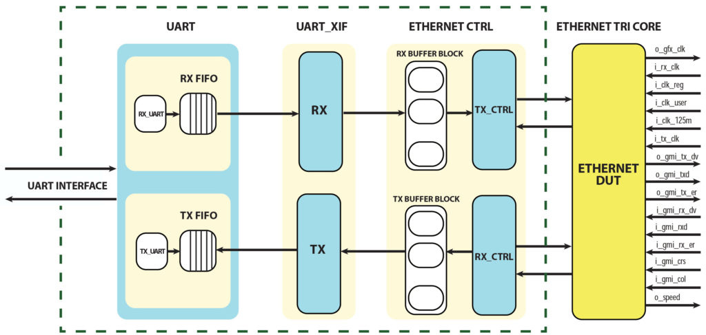
An Ethernet controller provides an example of how PSVIP can be used to provide a faster and more realistic way to validate prototype silicon or an FPGA programmed with the final design at speeds of up to 1 GHz. The validation setup includes the Ethernet controller PSVIP programmed onto the FPGA that in turn is controlled via a serial UART link on a Linux or Windows machine. The UART interface supports full-duplex communications for controlling the PSVIP. The driver can be based on a Perl script or optionally via a GUI and ship with a Perl driver.

A PSVIP can be used for an Ethernet Controller design to provide a faster and more realistic way to validate prototype silicon or an FPGA programmed with the final design at speeds of up to 1 GHz.
The UART interface above (see diagram) connects to a Linux computer or Windows PC via USB. The full-duplex–capable UART interface over USB is used for exchanging commands and responses between the PSVIP FPGA block and the test programs and driver running on the host Linux or PC machine.
Benefits associated with PSVIP instead of the traditional one-time, custom-built, post-silicon validation platforms often needed at the end of a design project are many. A PSVIP approach offers a reusable high-performance, standard platform used across numerous projects. It’s an alternative for fast and efficient verification and validation of standard interface protocols that is growing in popularity throughout the chip design and verification community.